Design and simulation
- Simulators: Finite element model (FEM) with COMSOL and mathematical studies with MathLab
- Layout tools: CAD / CleWin or ProEngineer
Substrate preparation / Substrate cleaning
- Plasma systems: O2 , CF4
- Polishing machine for chemical-mechanical polishing procedures (CMP)
- Chemical cleaning baths: Si, glass, optical materials
Structuring
- Photolithography: 365 nm exposure in proximity and vacuum contact, back exposure, DUV-flood exposure, Spin-/ Gyrset-Coater, Puddle developing
- Nanoimprint-Lithography (NIL)
- Selective wet chemical etching technique
- Dry etching processes: Reactive Ion Etching (RIE) , Kryo Inductively Coupled Plasma (ICP)
Materials synthesis
- Melt synthesis
- Powder production and processing
Coating / Diffusion
- Sputter systems: co-sputter systems, substrate heating up to 400°C
- Evaporation systems: electron-beam evaporator and thermal evaporator
- Material-/ inkjet printing
- Electroplating
- Diffusion and oxidation plants: dry and wet oxidation, temperature up to 1200°C
- Pulsed laser deposition (PLD)
Mounting and assembling technology
- Precision saw / wafer saw
- Ball / wedge bonders
- Welding unit: Resistance-, Wolfram-Inertgas (WIG) and ultrasonic welding
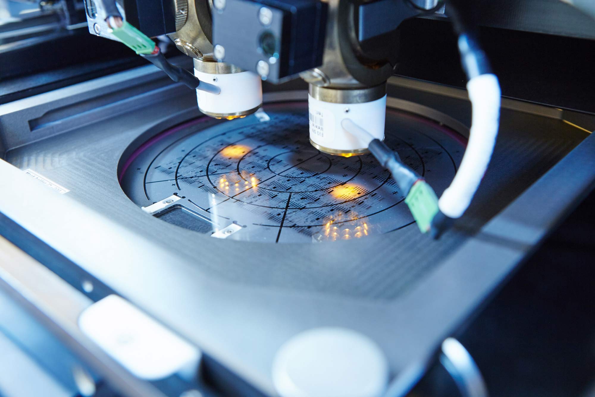
Structure and materials analysis
- Ellipsometry
- Profilometry
- Scanning electron microscope (SEM) with energy dispersive X-ray spectroscopy (EDX) and electron backscatter diffraction (EBSD)
- Computed Tomography (CT) with micro- and nanofocus
- Laser scanning microscope
- Measurement technology for the determination of thermoelectrical, optical and gas sensitive characteristics